- 您现在的位置:买卖IC网 > Sheet目录3876 > PIC16F1526-I/PT (Microchip Technology)MCU 14KB FLASH 768B RAM 64-TQFP
PIC16(L)F1526/27
DS41458B-page 46
Preliminary
2011 Microchip Technology Inc.
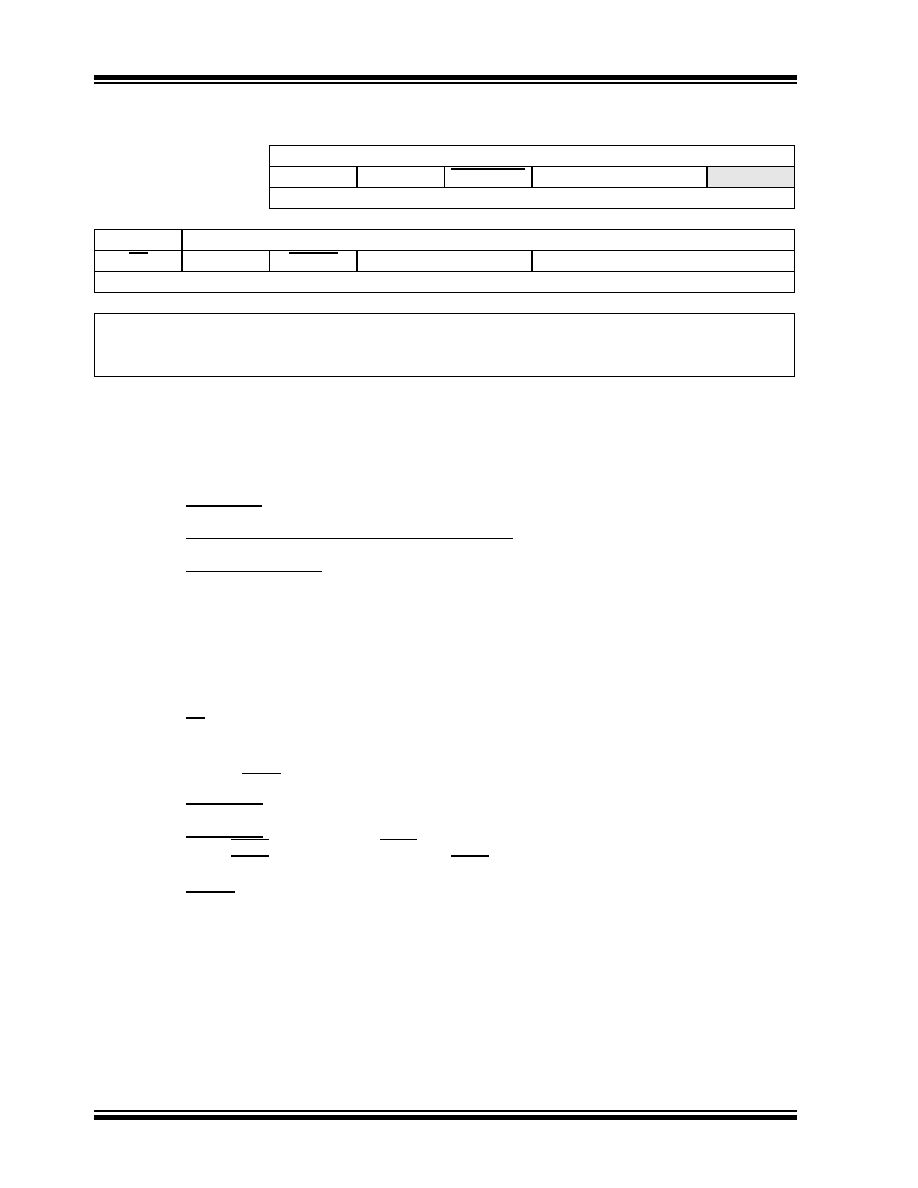
REGISTER 4-1:
CONFIGURATION WORD 1
R/P-1
U-1
FCMEN
IESO
CLKOUTEN
BOREN<1:0>
—
bit 13
bit 8
R/P-1
CP
MCLRE
PWRTE
WDTE<1:0>
FOSC<2:0>
bit 7
bit 0
Legend:
R = Readable bit
P = Programmable bit
U = Unimplemented bit, read as ‘1’
‘0’ = Bit is cleared
‘1’ = Bit is set
-n = Value when blank or after Bulk Erase
bit 13
FCMEN:
Fail-Safe Clock Monitor Enable bit
1
= Fail-Safe Clock Monitor is enabled
0
= Fail-Safe Clock Monitor is disabled
bit 12
IESO:
Internal External Switchover bit
1
= Internal/External Switchover mode is enabled
0
= Internal/External Switchover mode is disabled
bit 11
CLKOUTEN:
Clock Out Enable bit
If FOSC configuration bits are set to LP, XT, HS modes:
This bit is ignored, CLKOUT function is disabled. Oscillator function on the CLKOUT pin.
All other FOSC modes:
1
= CLKOUT function is disabled. I/O function on the CLKOUT pin.
0
= CLKOUT function is enabled on the CLKOUT pin
bit 10-9
BOREN<1:0>:
Brown-out Reset Enable bits
11
= BOR enabled
10
= BOR enabled during operation and disabled in Sleep
01
= BOR controlled by SBOREN bit of the BORCON register
00
= BOR disabled
bit 8
Unimplemented:
Read as ‘1’
bit 7
CP:
Code Protection bit
1
= Program memory code protection is disabled
0
= Program memory code protection is enabled
bit 6
MCLRE:
MCLR/VPP Pin Function Select bit
If LVP bit = 1:
This bit is ignored.
If LVP bit = 0:
1
=MCLR/VPP pin function is MCLR; Weak pull-up enabled.
0
=MCLR/VPP pin function is digital input; MCLR internally disabled; Weak pull-up under control of
WPUE3 bit.
bit 5
PWRTE:
Power-up Timer Enable bit
1
= PWRT disabled
0
= PWRT enabled
bit 4-3
WDTE<1:0>:
Watchdog Timer Enable bit
11
= WDT enabled
10
= WDT enabled while running and disabled in Sleep
01
= WDT controlled by the SWDTEN bit in the WDTCON register
00
= WDT disabled
发布紧急采购,3分钟左右您将得到回复。
相关PDF资料
PIC24F08KL401-I/SO
IC MCU 16BIT 8KB FLASH 20-SOIC
PIC18F13K50-I/MQ
IC PIC MCU FLASH 512KX8 20-QFN
PIC16F1934-I/PT
IC PIC MCU FLASH 256KX7 44-TQFP
PIC24F16KL402-I/SS
IC MCU 16BIT 16KB FLASH 28-SSOP
PIC16LF1934-I/PT
IC PIC MCU FLASH 256KX7 44-TQFP
PIC16C58B-20/P
IC MCU OTP 2KX12 18DIP
PIC18F24K20-I/SP
IC PIC MCU FLASH 8KX16 28-DIP
PIC16F1936-I/SP
IC PIC MCU FLASH 512KX14 28SPDIP
相关代理商/技术参数
PIC16F1526-I/PT
制造商:Microchip Technology Inc 功能描述:IC 8BIT MCU PIC16F 20 MHz 64-TQFP 制造商:Microchip Technology Inc 功能描述:IC, 8BIT MCU, PIC16F, 20MHz, TQFP-64
PIC16F1526T-I/MR
功能描述:8位微控制器 -MCU 14KB FL 768B RAM 10bit ADC 1.8-5.5V
RoHS:否 制造商:Silicon Labs 核心:8051 处理器系列:C8051F39x 数据总线宽度:8 bit 最大时钟频率:50 MHz 程序存储器大小:16 KB 数据 RAM 大小:1 KB 片上 ADC:Yes 工作电源电压:1.8 V to 3.6 V 工作温度范围:- 40 C to + 105 C 封装 / 箱体:QFN-20 安装风格:SMD/SMT
PIC16F1526T-I/PT
功能描述:8位微控制器 -MCU 14KB Flash RAM 768b nanoWatt
RoHS:否 制造商:Silicon Labs 核心:8051 处理器系列:C8051F39x 数据总线宽度:8 bit 最大时钟频率:50 MHz 程序存储器大小:16 KB 数据 RAM 大小:1 KB 片上 ADC:Yes 工作电源电压:1.8 V to 3.6 V 工作温度范围:- 40 C to + 105 C 封装 / 箱体:QFN-20 安装风格:SMD/SMT
PIC16F1527-E/MR
功能描述:8位微控制器 -MCU 28KB FL 1536B RAM 10bit ADC 1.8-5.5V
RoHS:否 制造商:Silicon Labs 核心:8051 处理器系列:C8051F39x 数据总线宽度:8 bit 最大时钟频率:50 MHz 程序存储器大小:16 KB 数据 RAM 大小:1 KB 片上 ADC:Yes 工作电源电压:1.8 V to 3.6 V 工作温度范围:- 40 C to + 105 C 封装 / 箱体:QFN-20 安装风格:SMD/SMT
PIC16F1527-E/PT
功能描述:8位微控制器 -MCU 14KB Flash RAM 768b nanoWatt
RoHS:否 制造商:Silicon Labs 核心:8051 处理器系列:C8051F39x 数据总线宽度:8 bit 最大时钟频率:50 MHz 程序存储器大小:16 KB 数据 RAM 大小:1 KB 片上 ADC:Yes 工作电源电压:1.8 V to 3.6 V 工作温度范围:- 40 C to + 105 C 封装 / 箱体:QFN-20 安装风格:SMD/SMT
PIC16F1527-I/MR
功能描述:8位微控制器 -MCU 28KB FL 1536B RAM 10bit ADC 1.8-5.5V
RoHS:否 制造商:Silicon Labs 核心:8051 处理器系列:C8051F39x 数据总线宽度:8 bit 最大时钟频率:50 MHz 程序存储器大小:16 KB 数据 RAM 大小:1 KB 片上 ADC:Yes 工作电源电压:1.8 V to 3.6 V 工作温度范围:- 40 C to + 105 C 封装 / 箱体:QFN-20 安装风格:SMD/SMT
PIC16F1527-I/MR
制造商:Microchip Technology Inc 功能描述:IC 8BIT MCU PIC16F 20 MHz 64-QFN 制造商:Microchip Technology Inc 功能描述:IC, 8BIT MCU, PIC16F, 20 MHz, 64-QFN; Controller Family/Series:PIC16F; Core Size:8bit; No. of I/O's:54; Program Memory Size:28KB; RAM Memory Size:1536Byte; CPU Speed:20MHz; Oscillator Type:External, Internal; No. of Timers:9 ;RoHS Compliant: No
PIC16F1527-I/PT
功能描述:8位微控制器 -MCU 14KB Flash RAM 768b nanoWatt
RoHS:否 制造商:Silicon Labs 核心:8051 处理器系列:C8051F39x 数据总线宽度:8 bit 最大时钟频率:50 MHz 程序存储器大小:16 KB 数据 RAM 大小:1 KB 片上 ADC:Yes 工作电源电压:1.8 V to 3.6 V 工作温度范围:- 40 C to + 105 C 封装 / 箱体:QFN-20 安装风格:SMD/SMT